3: Logic Circuits, Boolean Algebra, and Truth Tables
TOPIC 1: Logic Representation
There are three common ways in which to represent logic.
1. Truth Tables
2. Logic Circuit Diagram
3. Boolean Expression
We will discuss each herein and demonstrate ways to convert between them.
TOPIC 2: Truth Tables
A truth table is a chart of 1s and 0s arranged to indicate the results (or outputs) of all possible inputs. The list of all possible inputs are arranged in columns on the left and the resulting outputs are listed in columns on the right. There are 2 to the power n possible states (or combination of inputs). For example with three inputs there are 2^3=8 possible combination of inputs. (Audio)
TOPIC 3: Logic Diagram
A logic diagram uses the pictoral description of logic gates in combination to represent a logic expression. An example below shows a logic diagram with three inputs (A, B, and C) and one output (Y). The interpretation of this will become clear in the following sections.
Boolean Algebra can be used to write a logic expression in equation form. There are a few symbols that you’ll recognize but need to redefine.
 Note: Sometimes when the ! is used to represent the NOT it is used before the letter and sometimes it is used after the letter. Care should be used so that you understand which method is being used!
Below is an example boolean expression. In fact, it represents the same logic as the example logic circuit diagram above. This concept will also become clearer when we cover converting from and to the boolean expression below.
 TOPIC 5: Converting from a Logic Circuit Diagram to a Truth Table
This conversion is accomplished by selecting each state (or combination of inputs) one at a time, replacing the inputs with their respective values and figuring the value of each point through the circuit until the output is reached. The final output value for each state is then listed in the truth table next to the value of each input. Below is a logic circuit diagram with the input values. Study it carefully for an extended period of time, it is an animated image and the inputs and output will change every few seconds. (Click the image if it isn’t changing) Below are the results of the conversion in truth table form.
TOPIC 6: Converting Logic Circuit Diagrams to Boolean Expressions
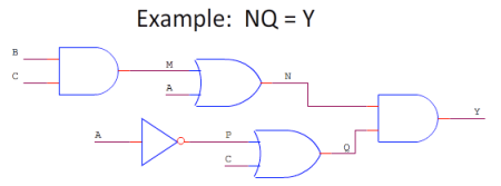
To convert from a logic circuit diagram to a boolean expression we start by listing our inputs at the correct place and process the inputs through the gates, one gate at a time, writing the result at each gate’s output. The following is the resulting boolean expression of each of the gates.
And here is an example of the process being carried out. The fact that the result simplifies to the XOR is merely coincidental. (Audio)

 TOPIC 7: Converting Truth Tables to Boolean Expressions
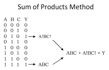
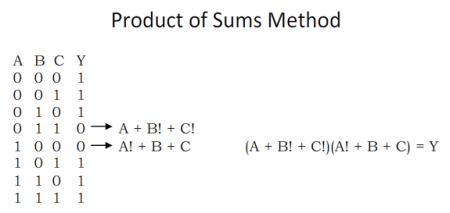
There are two methods for converting truth tables to boolean expressions.
The Sum of Products (Audio)
 The Product of Sums (Audio)

TOPIC 8: Converting Boolean Expressions to Logic Diagrams
Converting boolean expressions to logic diagrams is the most challenging conversion on this page because it requires a very good understanding of order of operation. Below is the order of operations used in this conversion. (Audio)
 In order to complete this conversion we will progress through the order of operations. We will first look for bracketed quantities or something in parentheses. Inside any parentheses we will look for more parentheses and then NOTs, then ANDs, then ORs. It’s best to begin with an example.
 Audio
Audio Audio
Audio Audio
Audio Audio
Audio TOPIC 9: Converting a Truth Table to a Logic Diagram
The easiest way to accomplish this is to first convert the truth table to a boolean expression and then to a logic diagram.
You should now be prepared to answer the following questions. Click here for Webct.
1. A logic system has 5 inputs. How many possible states exist in this system?
2. What symbol is used to represent the NOT gate when the line over the letter is not convenient to use?
3. A logic system has 3 inputs and therefore 8 possible states. The logic diagram representation is shown below. Complete the truth table and convert the output column to hexadecimal if the state 0 is the least significant bit and the state 7 is the most significant bit.
 4. Give the boolean expression from the above circuit diagram.
5. A truth table has the same states as in number 3 above. However, the output column from top to bottom reads 00110101. Give the result of the sum of products method.
6. Give the result of the product of sums method in number 5 above.
7. A boolean expression is given Y = (A+B)C+!BA+!C(A+B)+!(AC). Just as in 3 above, produce a truth table and convert the output column to hexadecimal.


September 15, 2010 at 9:52 pm |
In question number 3, I don’t understand what you mean by converting anything from a truth table into a hexadecimal figure. Could you give an example?
September 16, 2010 at 6:21 am |
If you take the output column (Y) and rotate it clockwise 90 degrees you’ll have a binary number such that the value of Y for state seven (A=1, B=1, C=1) is the most significant bit of the binary number and state zero (A=0, B=0, C=0) will be the least significant bit. For example, if the output column from top to bottom was 00011101 then the binary number would be 00011101 and would be equivalent to 1Dh. The same is true to question 7.
September 15, 2010 at 10:37 pm |
Did we learn how to convert a boolean expression into a truth table?
September 16, 2010 at 6:25 am |
You will need to apply the techniques of both TOPIC 5 and 8. Use TOPIC 8 to convert to a logic diagram and then TOPIC 5 to covert from a logic diagram to a truth table. Alternatively, you may take one state at a time and plug the values in to the boolean expression, work out the math and find the value of the output.
October 25, 2010 at 8:50 pm |
when converting boolean expression to boolean diagram how do u know when to tie the inputs to show that they share signals?
October 25, 2010 at 9:34 pm |
When you convert a boolean expression to a logic circuit diagram there is the possibility that there are more than one reference to the same input. You can tell from the boolean expression if this will be the case. If an input, say input A, occurs twice in the boolean expression then there will be two references to it in the logic circuit diagram. Because these are the same input they can be drawn as connected together and named once instead of twice. In my opinion I would rather have multiple references to the same input instead of a more complicated looking drawing but this is a matter of preference. Some may prefer to see only one reference to each input. Therefore, there is really no “right” answer only the happy-medium that they should be tied together and referenced once only if it does not complicate the drawing.
January 2, 2011 at 9:56 am |
If an math is (A!.B!).(C!.B!)!
Then what it’s Truth Tables & Logic circuit
January 2, 2011 at 11:44 am |
Mahfuz,
Start by simplifying. First use DeMorgan’s Theorem, i.e. (C!B!)=(C+B)!. Then use X!!=X to reduce to (A!B!)(C+B). Then distribute (or multiply through) to get A!B!C + A!B!B. Because B!B will always be zero you can simplify further to A!B!C. This should simplify the procedure of developing the logic diagram and truth table. Use the methods listed above for these.
Hope this helps.
March 15, 2011 at 9:22 pm |
can i please be helped how do we draw up the truth tabble from odd amounts of 1’s appear on three inputs to the logic circuit
April 8, 2011 at 7:30 am |
Begin by copying down all possible states. If there are three inputs then you’ll have 2^3=8 possible states. Now the output column will be a one if there are either one input or three inputs that are on. You should find four different outputs that are a 1. Hope that helps.
July 7, 2012 at 4:03 am |
please help me solve this problem!!! give the logic circuit diagram and complete true table of : a.) F=x’ y+y z’ (x y z) b.) G=a c+ b’ c+ a’ b
July 7, 2012 at 9:43 am |
On part a: when you multiply the first term through you get F=x’y + xyyzz’. By definition zz’=0 and the second term in the equation will always be zero so it simplifies to F = x’y + 0 = x’y. Using the simplified equation, obtain the table and circuit using the methods on the website. When it comes to the truth table you’ll need a column for z but its value will not impact the outcome (F). However, be careful… as your teacher may prefer you not simplify this in the way I did above. For part b, it should be relatively simple to use the methods on the website to get the table and circuit as this equation does not simplify easily. You’ll end up with two NOTs, three ANDs, and two ORs.
July 17, 2012 at 1:46 am |
how do you convert: truth table–>boolean equation–>logic circuit diagram if there is more than one output(y)?
July 17, 2012 at 4:57 am |
Consider them as completely separate problems each with their own singular outputs. So you’ll have one equation for each output and one diagram for each output. However, sometimes the logic diagrams can be simplified. For example if both equations contain the term AB’C then the circuit for that term could be drawn once and the output of that AND gate could be conected to two places, one in each diagram.
February 25, 2013 at 1:39 am |
HOW I CAN SIMPLIFY !A!B!C+!A!BC+A!BC+A!B!C+A!BC+ABC AND MAKE A CIRCUIT DIAGRAM? CAN YOU ANSWER THIS FOR ME?
February 25, 2013 at 6:48 am |
Richard,
Begin by factoring out !A!B from the first two terms to get !A!B(!C+C). Factor each of the remaining two sets of terms to arrive at similar results. You should now have three terms !A!B(!C+C) + … + … Remember that (!X+X) = 1 so the first piece simplifies to !A!B. After simplifying you’ll have !A!B + … + …, follow TOPIC 8 on my page to arrive at the diagram. Complete the NOTs(!) first then the ANDs and then the OR. You’ll end up with two NOT gates, three (two-input) AND gates, and one (three-input) OR gate.
Good Luck,
Adam
February 26, 2013 at 8:16 pm |
how it happens that (!x+x)=1?
in your topic 8 how about there is a nand’s, nor’s,exor’s, & exnor’s gate what is the order of operation?
February 27, 2013 at 12:44 pm |
Richard,
X!+X=1 can be shown by considering all possibilities; if X=1 then (0+1)=1, CHECK… if X=0 then (1+0)=1, CHECK… A similar story can be used to explain why X!X is always zero. Simplification is accomplished often times by factoring and realizing the boolean expression for more complicated gates (XOR for example) but a big component of simiplification is also to look at what is always true about an expression regardless of the value of the inputs. Many times it is these recognitions that ultimately lead to a realizable circuit diagram.
Regarding the order of operations when the higher level gates are involved: There are two ways to think about this, the first way is that all circuit diagrams representing boolean expressions CAN consist only of AND, NOT, and OR gates. Since it is possible to construct them as such, the logic diagram can then be examined for a simpler way to draw each subset of gates for example by replacing an OR gate followed by a NOT gate by a NOR gate. A second way of thinking about this is to keep the same order of operations as outlined in the material in TOPIC 8 but consider each of the additional gates in the category from which they get their name. That is, a NOR, XOR, and XNOR are all a variation of an OR gate and the NAND is a variation of an AND gate. Which way you look at it often depends on the type of system you are looking at and whether it has been “designed” as a problem in a book or it actually represents a real life system. I tend to think of things in the second method but it takes some care in how you examine the boolean expression. For example a NAND could be written as (AB)! or A!+B! so you need to recognize these expressions during the order of operations classification otherwise you’d identify the NOTs first, write them down, and never see the NAND until you draw an AND gate followed by a NOT. All this to say is that don’t proceed through the order of operations only one line at a time, i.e. don’t blindly go through and write out all of the NOTs before examining if there are any ANDs (or in this case NANDs). However, as a beginner it may be prudent to think things through in the first way and be able to recognize the circuit diagram of a NAND, NOR, XOR, and XNOR written with NOTs, ANDs, and ORs and make the simplification after the circuit is drawn.
It is interesting to note that often times designers will make an attempt to write the circuit using only NAND gates an excercise that is very worth while to learn in school. This exercise is actually meaningful because circuits are actually built, in some conventions, into silicon using only the NAND gate. The transistors that make up the gate lend themselves to fitting into place on the chip better than other gates.
Hope this helps,
Adam